Laserod s production division specializes in high resolution small spot size laser machining and silicon wafer resizing for semiconductor medical solar and microelectronics applications as well as patterning for the display industry.
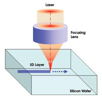
Laser dicing silicon wafer.
The minimum die dimension that the proposed method can achieve is 3 mm by 3 mm which in most cases meets the fabrication requirement of microfluidic chips.
Compared to industrial processes mechanical or already laser based dicing with ultra fast lasers promises material removal without damaging or weakening the surrounding material around the cut.
However laser ablation has its own problems.
Silicon wafer dicing blackstar wafer dicing system blackstar is a wafer dicing system utilizing fantom width laser dicing technology fwldt invented and patented by laser photonics and modified to accommodate the requirements of a silicon wafer singulation process without affecting the existent dicing method processes or procedures.
Svm wafer dicing capabilities.
Dicing of silicon wafers may also be performed by a laser based technique the so called stealth dicing process.
The chapter provides an overview about the laser dicing process of electronics substrates with the focus on silicon.
Laserod has a division that focuses on the building and integration of a full line of fiber laser micromachining equipment and a diode that can be used for laser dicing silicon wafer resistor trimming scribing substrates of silicon and alumina and cutting thin plastics and metals.
For silicon wafers less than 100 μm thick laser ablation offers an alternative to the blade technique which is too powerful for the delicate thin wafers.
Patterned and non patterned wafer substrates.
How is laser dicing silicon being processed.
The microdice laser micromachining system leverages tls dicing thermal laser separation a unique technology that uses thermally induced mechanical forces to separate brittle semiconductor materials such as silicon si silicon carbide sic germanium ge and gallium arsenide gaas into dies with outstanding edge quality while increasing manufacturing yield and throughput.
The same system can be used to downsize larger silicon wafers for use in smaller format processing tools.
Compared to dicing with a rotary saw or laser ablation the proposed method lowers equipment cost from more than 50 000 to 1 000 for silicon wafer dicing.
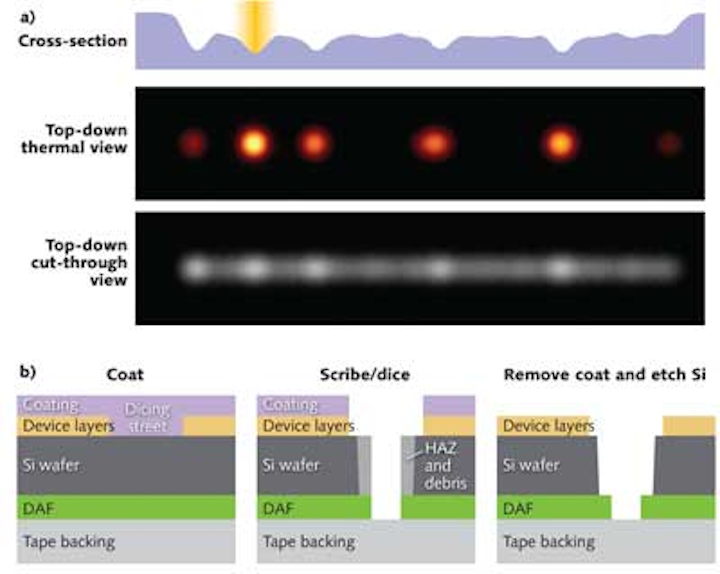
Vaporizing the wafer with a laser along the dicing path creates molten debris and microcracks.
Cut features are round holes with no cracking or rough edges.
It works as a two stage process in which defect regions are firstly introduced into the wafer by scanning the beam along intended cutting lines and secondly an underlying carrier membrane is expanded to induce fracture.
Dicing services are available for all wafer diameters ranging from 50mm to 300mm.
Demonstration of cutting features into 1 5 mm thick silicon wafers using a laser micromachining system equipped with a qcw laser.

.jpg)